SiC CVD
SiC CVD Process | SiC Ring | SiC Ring Manufacturing | LAON System & Equipment
SiC CVD Process introduction
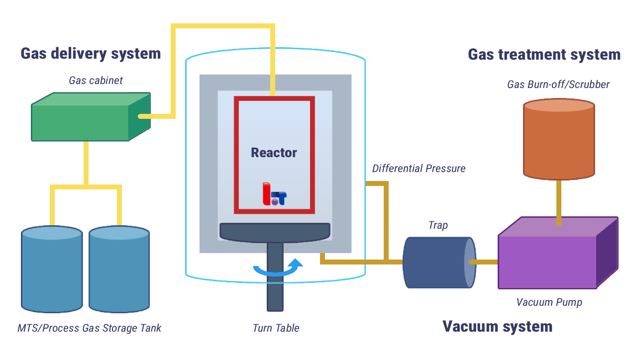
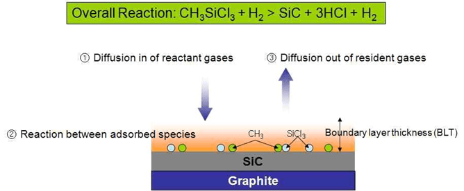
SiC CVD (Chemical Vapor Deposition of silicon carbide) – process, in which MTS (CH3SiCl3), a liquid SiC source, is vaporized with hydrogen and deposited on a ring-shaped graphite substrate to produce SiC Ring.
What SiC Ring is needed for?
Due to memory semiconductor stacking and miniaturization, dry etching time increases and the lifespan of internal chamber components decreases. The components with the shortest lifespan are ring-type components such as focus rings and guide rings.
Majority of production has moved from Si Ring and Quartz ring to SiC Ring for the following reasons:
– Increase in the number of NAND stacking layers. Demand for increased SSD capacity has driven the current stacking of 3D NAND to 200-300 layers. This is expected to increase to 500-600 layers within the next few years. The increased stacking requires an increase in the insulating layer (SiN/SiO2) that must be etched.
– Increased DRAM capacitor aspect ratio. Due to shrinking DRAM line widths, capacitor widths are also narrowing. Capacitor heights must increase to preserve capacity. Capacitor aspect ratios increase to over 100 in processes below 10nm.
The increased aspect ratio increases the contact depth that must be etched.

Problems with Si rings:
While still in use, their poor plasma resistance results in a short lifespan. This is especially true in high-power RF environments.
Future miniaturization and increasing complexity of semiconductor processes pushed Si rings to their limits (in terms of lifespan). Therefore, the adoption of SiC rings, a new material with long lifespan, is necessary. When comparing lifespans, SiC offers 1.5 times better plasma resistance than Si.
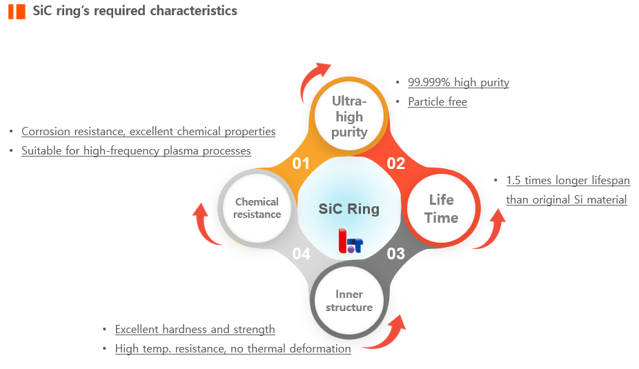
SiC rings characteristics:
– 0% porosity, uniform grain size
– Ultra-high purity SiC, superior quality
– Extended PM cycle: improved yield and reduced costs
SiC ring application fields:
- Semiconductor industry: Thin Film process, Etch process
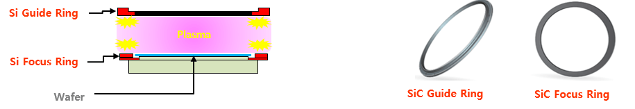
- Process equipment’s process kits: Focus Ring, Guide Ring, Shower Head
- Focus Ring or Edge Ring play important role for the uniformity and profile
- Etching of regular scope with the plasma attack causes amount of wafer to decrease
- Requires periodic change of consumable parts
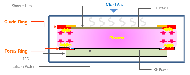
Etch Equipment inner structure
- Guide Ring: Plasma guide and Shower Head’s fixed role
- Shower Head: Covers wafer surface evenly with the process gas
- Focus Ring: Needed to focus plasma in a precise position/location
- ESC:
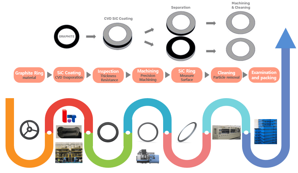
SiC Ring manufacturing process
LAON TMD has improved CVD equipment and process design for the effective SiC coating. You can learn more about LAON SiC CVD System characteristics in the page below.
LAON SiC CVD SYSTEM
Learn about a first-class SiC CVD System and results you can achieve with us.
REQUEST A QUOTE
You’re always welcome to ask us any questions. Submit your message here, and we will contact you soon.
Call or visit us : 09:00 ~ 18:00 (except Sat, Sun and public holidays)
TEL: 82-31-8077-2500 laontmd@laontmd.com 150-ho, 425, Doksanseong-ro, Osan-si, Gyeonggi-do, Republic of Korea, 18105